
GENTEN
Laser Repair for AR/VR Chips
Ultra-precision · Low thermal impact · High yield
Sub-micron precision processing with a 0.3 μm flat top beam for uniform energy distribution and minimal heat affected zone.
Discuss your application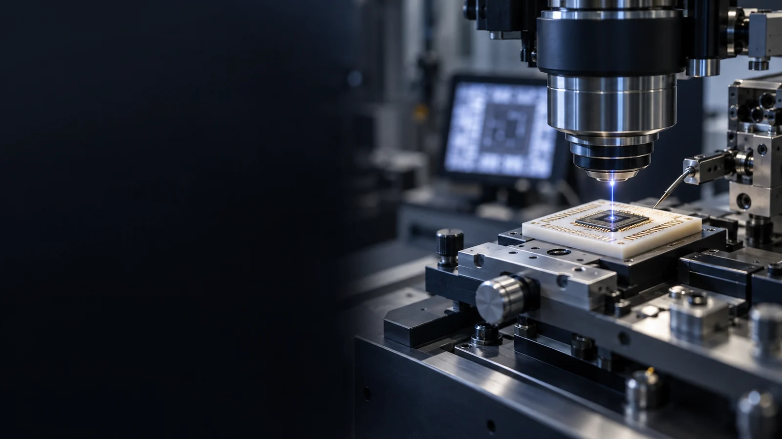
2 × 2 μmChip size
0.3 μmProcess spot size · Flat top
Sub-micronPositioning accuracy
Repair result
- Before repair (light leakage): the bright spot indicates light leakage, affecting display performance and contrast.
- After repair (dark non-emissive dot): successfully repaired as a dark non-emissive dot without affecting display performance.
Specifications
- Pulse duration — Ultra-short pulse
- Max. repetition rate — High speed
- Pulse energy — High efficiency
- Process spot size — 0.3 μm (Flat Top)
- Chip size — 2 × 2 μm
- Positioning accuracy — Sub-micron
- System integration — High compatibility
Beam profile
- Flat top beam profile
- 2D beam profile
- Line profile
Key features
- 0.3 μm flat top beam for uniform energy distribution
- Minimal heat affected zone to protect surrounding structures
- High precision positioning and stable process for 2 × 2 μm micro defect repair
- High repetition rate for productivity and high yield
Applications
- AR/VR microdisplay repair
- Micro LED repair
- Semiconductor repair
- Nano-structure processing
Equipment
- High precision laser platform
- High stability design
- High precision motion system
- Real-time vision alignment
- Auto focus control
- Safety interlock design
FROM CHALLENGE TO SOLUTION
Put precision to work.
Discuss your process with us.
Tell us what you’re working on. We’ll explore the right technology together.